
In terms of intelligent sensing and computing, this research center leverages our university's strengths in semiconductor and integrated circuit design.
We focus on the research and development of three key technologies: intelligent sensing systems, artificial intelligence computing chips, and robots and sensory synthesis.
From the sensing end, we extract important features and develop AI computing chips and systems through hardware-software co-design, achieving high-performance, rapid-response intelligent sensing and computing systems, which are applied to robotic perception.
Our forward-looking research goal is to develop high-performance intelligent sensing and computing chips.
For intelligent sensing chips, we utilize in-sensor computing to reduce data transmission requirements.
For intelligent computing chips, we employ non-Von Neumann architectures and in-memory computing technologies to achieve high energy efficiency computing chips at the POPs/W level.
By combining frame difference and area binarization, the chip enables the acquisition of both spatial and temporal features, which can be used for obstacle detection and avoidance. In the application of obstacle detection and avoidance, this spatial and temporal information allows for the calculation of dynamic stereo vision. Notably, this method is the first to calculate the depth of dynamic objects while filtering out the depth of static objects. The research result was published in IEEE Journal of Solid-State Circuits.
To overcome these challenges, our research group focuses on in-memory computing to break the memory wall and minimize data movement. In-memory computing reduces data transfer and energy consumption, providing a significant breakthrough in the circuit design . This approach contributes to the development of AI edge devices with constrained energy and hardware resources (see Figure B-5). In particular, our research group has developed various in-memory computing architectures tailored for different memory types (volatile and non-volatile). These architectures support fixed-point computing needs ranging from 1-bit to 8-bit, achieving world-leading energy efficiency in current in-memory computing technologies. Our research results were published in Nature Electronics, Proceedings of IEEE International Solid-State Circuits Conference (ISSCC), and Proceedings of IEEE Symposium on VLSI Technology and Circuits (VLSI Technology and Circuits).
Second, the Bit-Serial Cache leverages localized data caching to enhance performance and energy efficiency. It stores partial sums of recently computed input bit vectors, minimizing redundant computations through cache accesses. We introduce two new number formats: 1). BSFP (Bit-Serial Floating-Point), which approximates quantized floating-point numbers by linearly stacking multiple groups of two's complement integers. 2). FM-P2L (Fixed-Point to Linear), using fixed-point numbers for the highest significant bit and powers of two for the lowest significant bit. Detailed research findings were published in Proceedings of IEEE/ACM International Symposium on Microarchitecture (MICRO’23), Proceedings of International Conference on Learning Representations (ICLR’23), and Proceedings of ACM/IEEE Design Automation Conference (DAC’23).
To tackle these issues, we propose several innovative solutions. For example, we proposed block-based overlapped stripe inference for high-resolution image processing to reduce external memory bandwidth requirements. Utilizing structure-sparse kernel to decrease computational complexity at the same time with the use of a 40nm wafer to achieve a power efficiency of 4.6-8.3 TOPS/W, thereby to develop an ultra-high-definition 4K-UPVC chip which is capable of delivering high-quality images efficiently. Furthermore, we explore mixed-precision computing to reduce computational complexity. Our biased mixed-precision approach allows for 8-bit or 4-bit mixed-precision computing with only a 10% increase in area, saving 33% of power consumption while maintaining image quality. Research findings were published in IEEE Solid-State Circuits Letters, as well as Proceedings of Asia-Pacific Signal and Information Processing Association Annual Summit and Conference (APSIPA ASC).
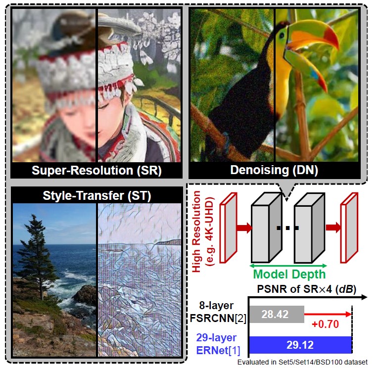
Figure B-10: Impact of Artificial Intelligence Computing Applications and Network Model Size on Quality
This application, termed a Triboelectric Nanosensor (TENS), detects analytes based on changes in electrical output influenced by adsorbed substances on the TENG's contact layer. While previous studies have explored TENS for sensing analytes like caffeine and pathogenic bacteria, few have demonstrated its potential for on-site detection critical in safety and environmental applications. In response, we propose integrating self-powered TENS with robotic hands for fingertip detection of mercury (Hg2+) ions. Conventional Hg2+ ion detection methods face challenges such as off-site detection, high power consumption, complex sample preparation, and lengthy processing times. Our solution involves a tellurium nanowire-based self-powered TENS capable of selectively detecting Hg2+ ions. Integrated with a robotic hand, the TENS comes into contact with and separates Hg2+ ion solutions, altering triboelectric output due to substance-specific triboelectric polarity. Real-time output signals are wirelessly transmitted via a Bluetooth system integrated into the robotic hand to a smartphone, demonstrating on-the-spot detection of Hg2+ ions in real samples. Research finding was published in ACS Nano.
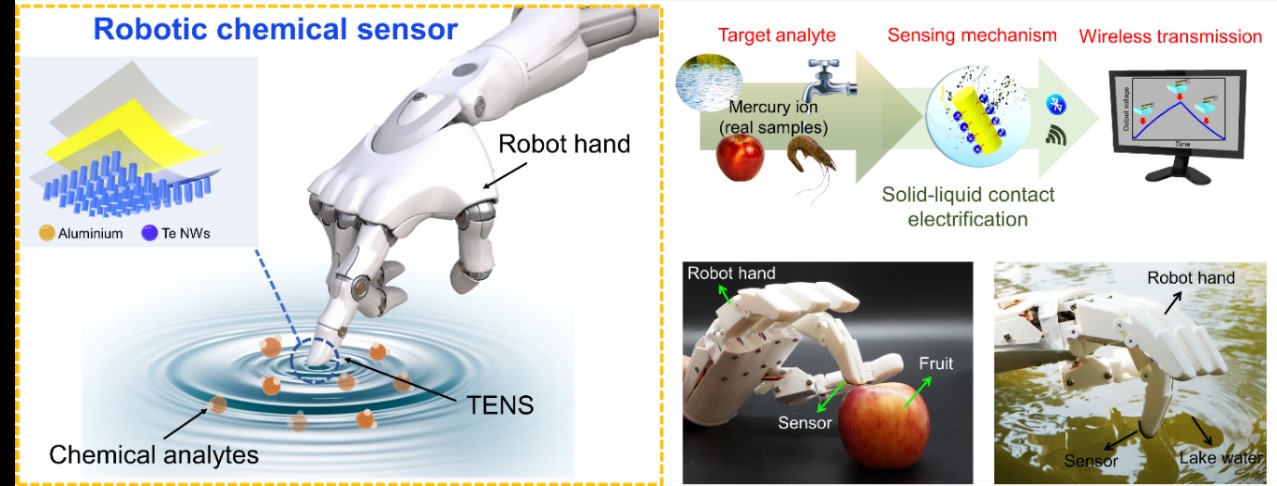
Figure B-11, Friction Nanosensor
Additionally, to ensure safe human-robot interactions, we developed soft material-actuated robot fingers. Traditional soft robot fingers often lack precise control over fingertip positions, so we introduced innovative Modular Soft Actuators (MSA). These MSAs offer both adaptive behavior and precise joint angle control for anthropomorphic robot fingers. Each air chamber's pressure is independently controlled, allowing for more accurate joint angles compared to traditional PneuNets soft actuators. A rigid skeleton enhances force transfer and measurement capabilities, ensuring each module can effectively withstand and transfer forces during use. Experimental results demonstrate that the modularized soft actuator performs exceptionally well and is adaptable to various applications. The research results related to robotic finger drive mechanisms were published in ASME Journal of Mechanisms and Robotics, Proceedings of the 2023 IET International Conference on Engineering Technologies and Applications (IET IECTA 2023), and Proceedings of the IFTOMM World Congress (IFToMM WC2023).
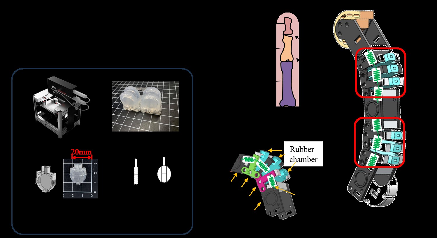
Figure B-12, Modular Flexible Actuator Finger Structure.
By combining frame difference and area binarization, the chip enables the acquisition of both spatial and temporal features, which can be used for obstacle detection and avoidance. In the application of obstacle detection and avoidance, this spatial and temporal information allows for the calculation of dynamic stereo vision. Notably, this method is the first to calculate the depth of dynamic objects while filtering out the depth of static objects. The research result was published in IEEE Journal of Solid-State Circuits.
To overcome these challenges, our research group focuses on in-memory computing to break the memory wall and minimize data movement. In-memory computing reduces data transfer and energy consumption, providing a significant breakthrough in the circuit design . This approach contributes to the development of AI edge devices with constrained energy and hardware resources (see Figure B-5). In particular, our research group has developed various in-memory computing architectures tailored for different memory types (volatile and non-volatile). These architectures support fixed-point computing needs ranging from 1-bit to 8-bit, achieving world-leading energy efficiency in current in-memory computing technologies. Our research results were published in Nature Electronics, Proceedings of IEEE International Solid-State Circuits Conference (ISSCC), and Proceedings of IEEE Symposium on VLSI Technology and Circuits (VLSI Technology and Circuits).
Second, the Bit-Serial Cache leverages localized data caching to enhance performance and energy efficiency. It stores partial sums of recently computed input bit vectors, minimizing redundant computations through cache accesses. We introduce two new number formats: 1). BSFP (Bit-Serial Floating-Point), which approximates quantized floating-point numbers by linearly stacking multiple groups of two's complement integers. 2). FM-P2L (Fixed-Point to Linear), using fixed-point numbers for the highest significant bit and powers of two for the lowest significant bit. Detailed research findings were published in Proceedings of IEEE/ACM International Symposium on Microarchitecture (MICRO’23), Proceedings of International Conference on Learning Representations (ICLR’23), and Proceedings of ACM/IEEE Design Automation Conference (DAC’23).
To tackle these issues, we propose several innovative solutions. For example, we proposed block-based overlapped stripe inference for high-resolution image processing to reduce external memory bandwidth requirements. Utilizing structure-sparse kernel to decrease computational complexity at the same time with the use of a 40nm wafer to achieve a power efficiency of 4.6-8.3 TOPS/W, thereby to develop an ultra-high-definition 4K-UPVC chip which is capable of delivering high-quality images efficiently. Furthermore, we explore mixed-precision computing to reduce computational complexity. Our biased mixed-precision approach allows for 8-bit or 4-bit mixed-precision computing with only a 10% increase in area, saving 33% of power consumption while maintaining image quality. Research findings were published in IEEE Solid-State Circuits Letters, as well as Proceedings of Asia-Pacific Signal and Information Processing Association Annual Summit and Conference (APSIPA ASC).

Figure B-10: Impact of Artificial Intelligence Computing Applications and Network Model Size on Quality
This application, termed a Triboelectric Nanosensor (TENS), detects analytes based on changes in electrical output influenced by adsorbed substances on the TENG's contact layer. While previous studies have explored TENS for sensing analytes like caffeine and pathogenic bacteria, few have demonstrated its potential for on-site detection critical in safety and environmental applications. In response, we propose integrating self-powered TENS with robotic hands for fingertip detection of mercury (Hg2+) ions. Conventional Hg2+ ion detection methods face challenges such as off-site detection, high power consumption, complex sample preparation, and lengthy processing times. Our solution involves a tellurium nanowire-based self-powered TENS capable of selectively detecting Hg2+ ions. Integrated with a robotic hand, the TENS comes into contact with and separates Hg2+ ion solutions, altering triboelectric output due to substance-specific triboelectric polarity. Real-time output signals are wirelessly transmitted via a Bluetooth system integrated into the robotic hand to a smartphone, demonstrating on-the-spot detection of Hg2+ ions in real samples. Research finding was published in ACS Nano.

Figure B-11, Friction Nanosensor
Additionally, to ensure safe human-robot interactions, we developed soft material-actuated robot fingers. Traditional soft robot fingers often lack precise control over fingertip positions, so we introduced innovative Modular Soft Actuators (MSA). These MSAs offer both adaptive behavior and precise joint angle control for anthropomorphic robot fingers. Each air chamber's pressure is independently controlled, allowing for more accurate joint angles compared to traditional PneuNets soft actuators. A rigid skeleton enhances force transfer and measurement capabilities, ensuring each module can effectively withstand and transfer forces during use. Experimental results demonstrate that the modularized soft actuator performs exceptionally well and is adaptable to various applications. The research results related to robotic finger drive mechanisms were published in ASME Journal of Mechanisms and Robotics, Proceedings of the 2023 IET International Conference on Engineering Technologies and Applications (IET IECTA 2023), and Proceedings of the IFTOMM World Congress (IFToMM WC2023).

Figure B-12, Modular Flexible Actuator Finger Structure.


